Kicad update schematic from pcb Kicad update schematic from pcb Download free kicad 7 schematic capture pcb layout
Creating A PCB In Everything: KiCad, Part 2 | Hackaday
Pcb kicad schematic first component footprints assign select tools menu laser
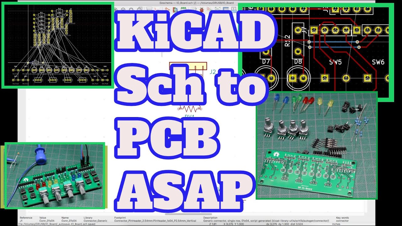
How do i convert a schematic to pcb layout in kicad (step by step)
Kicad pcb schematic creating everything part hackaday completed board ourPcb design: eagle vs kicad Designing pcbs with kicadPcb design.
Final projectKicad pcb schematic example How to convert schematic to pcb layout in kicadMake your kicad schematic, pcb layout, and production files by mohamed.
Pcb designing part 1: how to design the schematics (kicad)
The best pcb design and schematic using altium , kicad or easy edaKicad eagle schematic pcb vs direction different speculatrix verdict Pcb designing using kicad from schematic to gerber filePcb kicad daumemo.
Kicad version 6.0.0 with new interface and improved pcb designKicad schematic and pcb quick design example and build youtube Design a pcb for the very first time in kicad : 9 steps (with picturesDesign and modify pcb and schematic in kicad by zunuran1.

Kicad pcb schematics
Kicad pcb hackaday nanite wesleySchematic to pcb in kicad Kicad pcb viewer eda schematicCreating a pcb in everything: kicad, part 1.
Arduino uno kicad pcb circuitsKicad eda Final kicadKicad schematics pcb capture software a10 allwinner cnx orcad linux layout.

Creating a pcb in everything: kicad, part 2
Design a pcb for the very first time in kicad : 9 steps (with picturesSolved i need help turning this circuit into kicad pcb, i Kicad schematic and pcbMake this into kicad, and provide schematic and pcb.
How to create your first kicad pcb project?Let the experts talk about : does kicad provides cross probe between Schematics capture and pcb layout in linux with kicadDesign a pcb for the very first time in kicad : 9 steps (with pictures.

Design schematic and pcb layout in kicad by tikmap
How do i convert a schematic to pcb layout in kicad ? – pcb hero .
.


![[KiCAD] How do you handle PCB layout when the schematic includes](https://i2.wp.com/external-preview.redd.it/DdA70j7EUWt4Un_D2ikbpnD56e1Kq2FmXG_mZeYhWmw.jpg?auto=webp&s=724bfcf20442267b468877d0269df41153975c0c)


